Lesson 010 - VCO
and AGC AMP
THE MOST DIFFICULT CIRCUIT IN THE
MP20.
YOU GET THIS BUILT & THE REST IS DOWNHILL....
Please use version 1.5 of the PLL drawing as a reference.
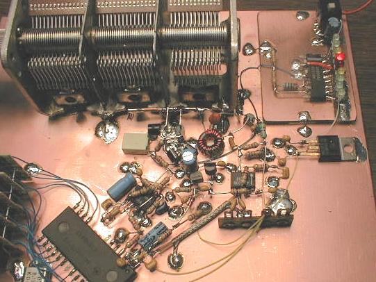
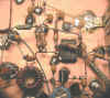
This lesson may look hard, but it's
just 1 part soldered at a time - no big deal - just go slow. See the above
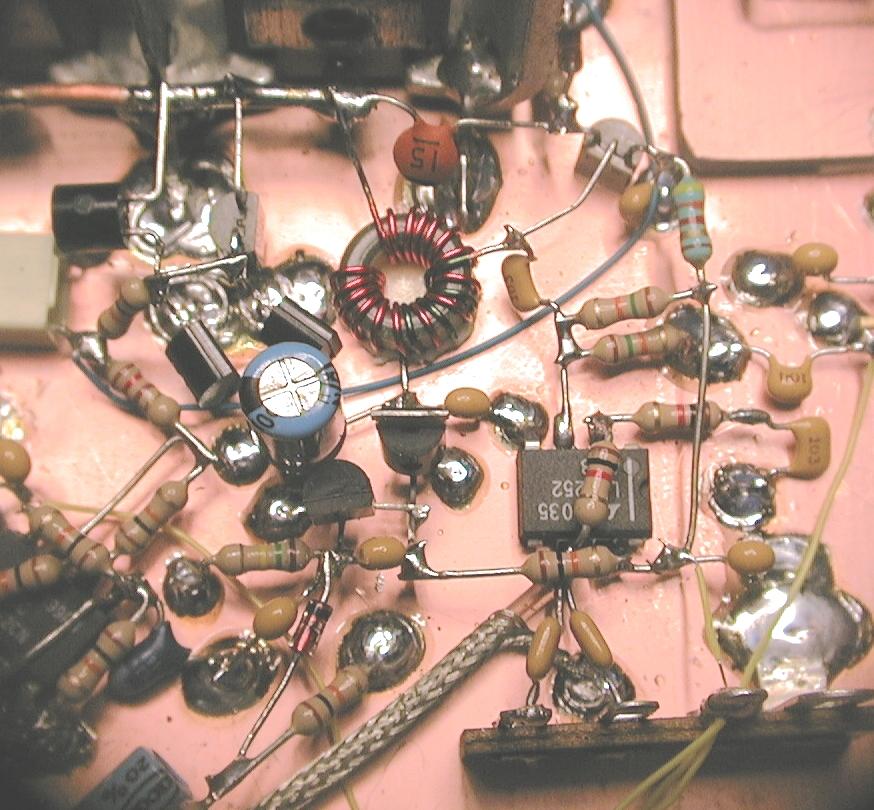
picture and the schematic as reference for parts layout.
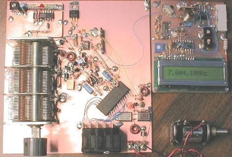
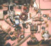
This is a picture of the
completed PLL with the FC adjacent to it on the right.
I have it here to give you a perspective of the PLL
Solder a 10k resistor (R12) to C15, the 470pF square cap.
At this point, get C25, a varicap that should give a value of 365 pF or larger.
If you do not have a vari-cap, then we need another part as a place holder for
the varicap. I suggest you use a spare junk capacitor that has a value of
500 pF or less. Connect the four MV209 varactors (D3-D6) between ground,
the free end of R12 and the varicap (C25). Connect all the cathodes to
R12. The cathode on the MV209 is identified as follows: Hold the MV209
with the flat side facing you and the leads pointing down. The cathode is the
lead on the right.
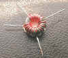
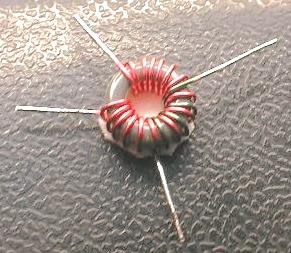
Prepare L4, the tuning inductor for the VCO. Tightly wind 16 turns on a
yellow T37-6 toroid. Clip any excess leads to 1/2 inches and stip and tin.
Wind 4 turns over the middle of the primary turns. Cut to 1/2 inch, strip
and tin. Place some double stick tape on the bottom of the inductor.
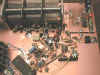
The final product should look EXACTLY like the picture. It is CRITICAL that the
windings are as in the picture. The schematic shows two dots on the bottom
of L4. These represent the phasing of the windings. It the phasing
is reversed on one of the windings, the VCO will not oscillate.
Position L4 as in the pictures and
solder the 16 turn winding wires to the varicap and ground. Solder the 15 pF
(C16) cap to the varicap. Next, solder the GATE of Q2 (J310) to the other end of
the 15 pF cap. Solder the SOURCE pin to the 4 turn winding on L4. Use the
pictures as a guide. Solder a 100 nF cap (C17) from the DRAIN of Q2 to ground
Solder a 10n cap (C18 to the source pin on Q2. Install resistors R14,R15 and
R16. Prep the pins on the video amp (U4). Solder pin 4 to ground per the
picture.
NOTE: pins 1,5 and 8 are
broken off, as they are not used. Install R17, R18 and C20. Connect a 10n
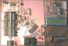
cap (C27) to pin 6 on U4. Connect the other end to a Manhattan pad or a
terminal strip as in picture 14. This will go to a mixer on the xcvr board.
Connect C7 from pin #1 on the PLL (U1) to pin 6 on U4.
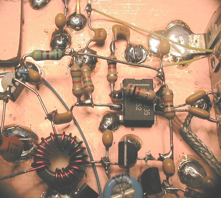
Solder the remaining components to the LM1252 (U4)
videoamp. Use the pictures as a reference.
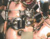
Place a 7808 voltage regulator as
show in the picture. Solder the tab and the center pin to the copper
board. Connect a 100 nF cap to both the remaining pins to ground.
Look at picture 16, Connect the lower pin of the regulator to all the power
points on the PLL board. They are:
a. DRAIN on Q1
b. pin #3 on the PLL U1
c. pin 8 on U2
d. pin 7 on U4
Also check R19 and P1 (the tune pot)
The upper pin on the 7808 voltage regulator goes to a 12 volt supply.
Double check all connection and make sure nothing is missing. If you apply
power to the PLL, the circuit will (should) draw about 50 milliamps.
NOTE: The mosfet, Q3 is in a plastic bag in the tranceiver
kit. The pinout is as follows:
Hold the mosfet number side towards you with the pins down. The SOURCE pin is to
your left and the GATE pin is in the center. So
where is the DRAIN pin?
END OF LESSON 10 - NEXT IS THE PLL TESTING and
"understanding the PLL"
Back to Lessons
Page