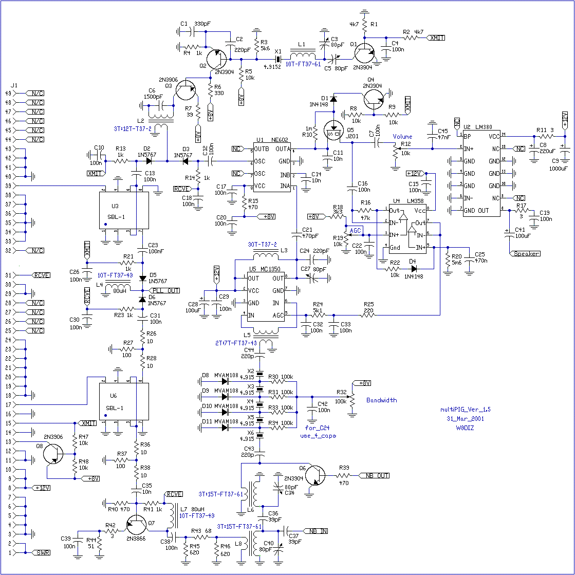
1. Start with a 6 x 6 inch square copper board or larger.
Lesson 014 , Transceiver Construction
OK...here we go...use the LATEST
SCHEMATIC as a reference...
![]()
![]()
1. Start with a 6 x 6 inch square copper board or larger.
Actual minimum size is 6 x 4 but 7 x 5 can't hurt. My board is 6 x 6. Obtain a used PC 16 bit ISA socket.
I got mine from a surplus 486 motherboard. Used a propane torch to remove the sockets. Works great. No damage.
Position a socket on the copper board as shown in pix#1. On the lower set of contacts/pins, bend some of pins at right angles.
The right angle pins are #1,2,8,9,10,13,15,17,31 and 39.
See pix#2 and #3. Solder ALL the unbent pins to the copper board.
See the pictures as a reference. When all the pins are soldered, the socket will remain secured to the copper board, while inserting
a 16 bit ISA card.
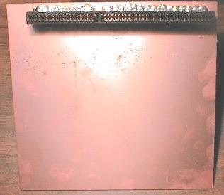
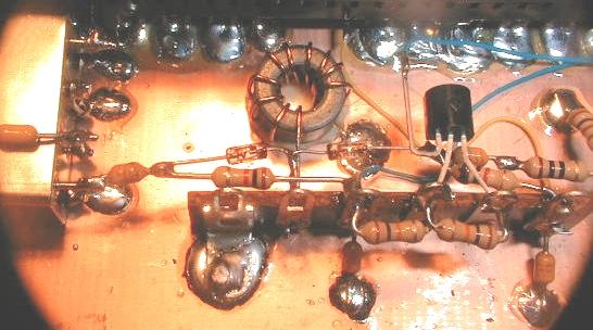
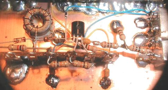
2. Build up the 2 SBL-1 mixers. The BLUE dot represents pin #1.
Pin #2 is across from pin #1. The pinout is depicted on the schematic.
Prep the mixers by soldering a jumper from pins #5 and #6. Solder on grounding pigtails to pins according to the schematic. Also place a jumper with a pigtail from #3 and #4. See pics #4,5,6,7. Be aware that on the SBL-1, PINS 1 and 2 are interchangeable, as are pins 7 and 8.
PAY CLOSE ATTENTION HERE
As an example, the schematic shows U3 with pin #1 going to ground and pin #2 goting to socket pin #39. I could have grounded pin #2 and connected pin #1 to the socket pin #39.
Position U3 (SBL-1) so that pin#1 and #2 are opposite the socket pin#39. Solder U3's grounding wires as seen in pix#5. solder a 3 inch long 30 gauge wires on the sockets pins #31, #15 and #13.
Position U6 (SBL-1) so that pin#1 and #2 are opposite the socket pin#17. Solder U6's grounding wires as seen in pix#5.
![]()
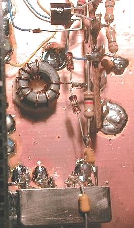
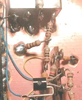
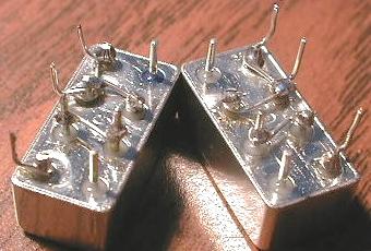
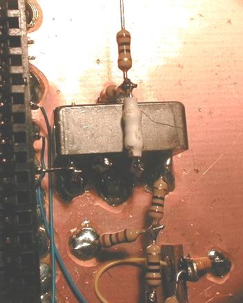
3. In the middles of pix#7, I show a 6 pin solder lug with a ground
lug on the left side. From left to right in pix#7, the lugs are GROUND, PLL OUT, XMIT, base of Q8, +8V,
RCVE.
PLL OUT goes to the PLL board. XMIT goes to pin #15, RCVE goes to pin #31. The +8 volts is on the T/R switch schematic. Solder 100 nF caps (C26, C30) from lugs XMIT and RCVE to ground. Prep L4 with 10 turns of #24 or #26 wire. Use the thicker black toroids. Mount some double sick tape on the toroid, strip and tin the wires and position it next to and between pins #31 and #32. Solder one toroid lead to ground.
Solder 100 nF caps (C13, C23) as shown in pix#7. Solder the T-network to pins 4/5 on U6, (R36,R37,R38). R36 has a small piece of heat shrink tubing on it to prevent it shorting to the case on U6. Solder another T-network to pin #8 of U6 (R26,R27,R28). Solder a 100 nF cap (C31 ) to the end of R26.
Connect the pin diodes D5 and D6 (the clear colored diodes) to the end of C31 and C23. Solder R21 from the XMIT lug to the ANODE of D5. Solder R23 from the RCVE lug to the ANODE of D6. Solder the XMIT wire from pin #15 to the XMIT lug.
Solder the RCVE wire from pin #31 to the RCVE lug. Solder the 10k resistors, R47 and R48 to lugs as shown in the picture. Get Q8, a 2N3906 and bend the collector pin as show in the pictures. Solder the base to the junction of the 2 10k resistors R47,R48 and solder the EMITTER to the lug named +8V. Make sure that everything is soldered and that your work looks like the pictures.
DOUBLE CHECK EVERYTHING NOW.
Later it becomes difficult to fix things as
this board will get crowded.
END OF LESSON #014