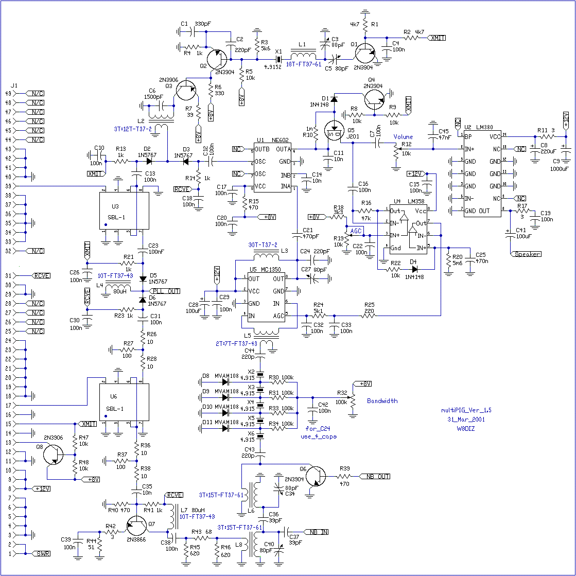
along with the schematic. Figure out the best parts placement.
Make sure you can fit everything per the schematic.
1.
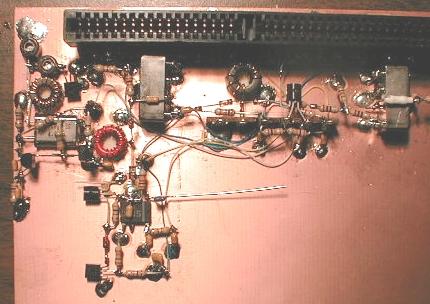
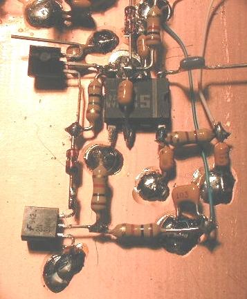
Here is a picture of the BFO and the IF-CW detector,
that were added since lesson #014. Notice that there
are parts right up to the edge of the board.
2.
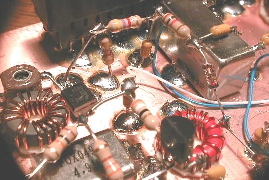
Solder the PIN diode D2 and R13 (1k) to the cap (C13)
coming over the top of SBL-1 (U3). Next solder the bias resistors
R1 and R2 (4k7) as shown in the picture. Use C10 to support R13 and R2.
Solder C4 from the junction of R1 and R2 to ground. Solder in Q1, a 2N3904.
3.
Bend the connecting pin UP on one of the Brown vari-caps. Solder the
pin on the round side of the cap (C5) to the collector of Q1. See Pix.
Solder another vari-cap (C3) from C5 to ground EXACTLY as in the picture.
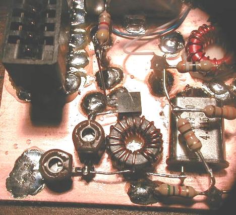
Wind 18 turns on a FT37-61 toroid (the smaller black ones). Strip and tin.
Secure to the copper board using double stick tape. Solder on end to the
junction of C3 and C5. Connect the other end of L1 to the BFO xtal.
This xtal is in a bag all by itself.Connect as shown in the pix.
Solder the case of the xtal to the copper board.
Connect a 5k6 resistor (R3) from the other leg of the xtal to ground.
4.
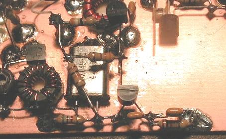
Solder C1 (330pF) and C2(220pF) and R4 (1k) as shown in the picture.
Bend the leads up on a 2N3904 (Q2) and solder the emitter and base as
shown in the picture. Use your schematic here. Solder R5 (10k) and R6 (330)
Solder in Q3 and R7. Connect the free ends of R7, R6 and R5 to a 100nF cap
to ground. This 100nF cap is not in the schematic but is supplies as an extra.
Repeat...from the junction of R5,6,and 7 connect a 100nF cap to ground.
Connect C6, a small yellow cap labeled "152" and connect to L4, Q3 and ground.
Make sure that all parts associated with Q1, Q2 and Q3 are soldered in place.
This completes the BFO oscillator.
5.
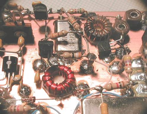
Solder D3, C12, R14, and C18 per the pictures and schematic. Straighten the pins
on U1, a NE602 or sub device. Break off pins 5 and 7. Solder the end of C12 to pin
#6 on U1. Solder the ground pin #3. Solder C17 and R15 to pin #8 on U1. Solder C20
to the free end of R15 and to ground. Solder C14 from pin2 to ground. Solder C21,
a 470 pF blue cap to pin #1 and let the free end float. See the pix.
Solder C11, a 10nF cap from pin 4 to ground. Form the leads on the J201 FET as in
the pictures. Solder the source pin of J201 to pin 4 of U1. Solder D1 to the gate
of J201 and then connect the other end of D1 to Q4's collector. Solder Q4's emitter
to ground. Solder R10 from pin 4 of U1 to the gate of Q5, the J201 FET.
Solder R8 and R9 to the base of Q4. Solder the free end of R8 to ground. Solder the
free end of R9 to a spare cap 10nF or 100nF for for support (to ground).