Lesson 008 - More PLL
Construction
PLL Construction - Ref. Oscillator plus ADDENDUM
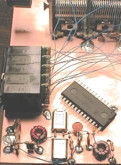
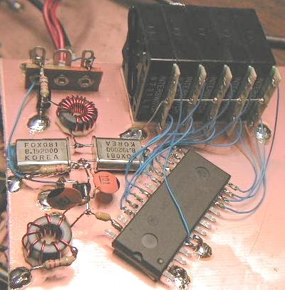
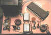
1. Remove the protective paper from the double stick tape on the octal
switches and mount it 1.4 inches from the side as seen in the picture #5.
Solder the solid conductor [running thru hole "A" on the switches] to
the copper ground plane.
2. On the PLL schematic, you will see P1, P2 and P3. These pads
connect to the main tune 10 turn freq control pot. We need to create these pads
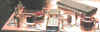
on the copper board. Either obtain a terminal strip as seen in the picture
#6 or make up some "manhatten" pads. I prefer the terminal strips.
3. Connect a 10K resistor to the terminal strip and solder. Connect the
MV209 diode from the 10K resistor to the copper ground plane as showmn in the
picture. The flat side of the diode is facing you in the picture.
4. Find the smaller of the two black toroids in the PLL kit. Using
#24 or #26 wire, tightly wind 18 turns of wire on the toroid. This is the
FT37-61. Cut any excell wire tails, leaving 1/2 inch of wite tail.
Strip and tin the tire tail. Next, cut a piece of double stick tape 0.5 x 0.5
inches. Stick it on one side of the wound toroid. Remove the plastic
paper from the other side of the tape and mount the toroid as shown in picture
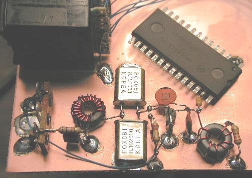
#5. Find the 2 8.192 MHz xtals and trim the leads to 1/4 inch. Place the
xtals flat on the copper board as shown in the picture #5 and solder the top of
the xtals to the copper. Make sure the xtal leads are in-line so they can be
soldered together as shown in the schematic.
5. Form the J310 FET as shown in picture #8. Solder the GATE to the
XTALS. Connect the DRAIN to a 100nF cap C4. Solder the other end of
C4 to ground. Make a network by connecting in parallel a 1N4148 diode and
a 220k resistor. Solder the ends together. The banded end of the diode
goes to ground. Connect the 100pF cap across the J310's GATE and SOURCE.
Connect a 150 pF from J310's SOURCE to ground. Wind 8 turns #24 or #26 wite onto
the larger of the 2 black toroids. Use a small piece of double stick tape
on the bottom of the toroid. Strip and tin the leads and mount the toroid
L2 as in the pictures. SOlder a 100 nF cap at the junction of J310 SOURCE
and L2.

6. Straighten out all the pins on the MC1345151P2 PLL chip EXCEPT pin 2.
Clip the legs from all the straightened pins as shown in pictures. Place a
small strip of double stick tape on the bottom of the PLL chip. Mount the
chip so that C5 aligns with PIN #27
on the PLL. See the pictures as an example. Solder C4 to pin 27. Solder
pin 2 to ground. Place a small wire to PIN 6 on the PLL and solder to
ground.
7. Connect all the leads from the octal switches to the PLL as follows:
the switches from right to left,
connect 1 on
the switch to pin 11 on the PLL
connect 2 on the switch to pin 12 on the PLL
connect 4 on the switch to pin 13 on the PLL
using the 2nd switch from the right
connect 1 on the switch to pin 14 on the PLL
connect 2 on the switch to pin 15 on the PLL
connect 4 on the switch to pin 16 on the PLL
using the left switch (or middle if you have 5 switches
connect 1 on the switch to pin 17 on the PLL
connect 2 on the switch to pin 18 on the PLL
connect 4 on the switch to pin 19 on the PLL
if you have 4 switches then
connect 1 on the switch to pin 20 on the PLL
connect 2 on the switch to pin 24 on the PLL
connect 4 on the switch to pin 25 on the PLL
if you have 5 switches then
connect 1 on the switch to pin 22 on the PLL
connect 2 on the switch to pin 23 on the PLL
connect 4 on the switch to pin 5 on the PLL
ADDENDUM STARTS HERE:
NOTE: If you do not have 5 octal switches, connect a set
of DIP switches to pins
20,24,25,22,23,and 5 IN THAT ORDER.
The other sides of the dip switches go to ground.
END OF LESSON 8 and ADDENDUM
Back to Lessons
Page